Disorder in van der waals heterostructures of 2d materials
Disorder in van der waals heterostructures of 2d materials"
- Select a language for the TTS:
- Dutch Female
- Dutch Male
- Language selected: (auto detect) - NL
Play all audios:
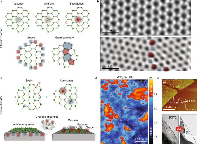
ABSTRACT Realizing the full potential of any materials system requires understanding and controlling disorder, which can obscure intrinsic properties and hinder device performance. Here we
examine both intrinsic and extrinsic disorder in two-dimensional (2D) materials, in particular graphene and transition metal dichalcogenides (TMDs). Minimizing disorder is crucial for
realizing desired properties in 2D materials and improving device performance and repeatability for practical applications. We discuss the progress in disorder control for graphene and TMDs,
as well as in van der Waals heterostructures realized by combining these materials with hexagonal boron nitride. Furthermore, we showcase how atomic defects or disorder can also be
harnessed to provide useful electronic, optical, chemical and magnetic functions. Access through your institution Buy or subscribe This is a preview of subscription content, access via your
institution ACCESS OPTIONS Access through your institution Access Nature and 54 other Nature Portfolio journals Get Nature+, our best-value online-access subscription $29.99 / 30 days cancel
any time Learn more Subscribe to this journal Receive 12 print issues and online access $259.00 per year only $21.58 per issue Learn more Buy this article * Purchase on SpringerLink *
Instant access to full article PDF Buy now Prices may be subject to local taxes which are calculated during checkout ADDITIONAL ACCESS OPTIONS: * Log in * Learn about institutional
subscriptions * Read our FAQs * Contact customer support SIMILAR CONTENT BEING VIEWED BY OTHERS BANDGAP ENGINEERING OF TWO-DIMENSIONAL SEMICONDUCTOR MATERIALS Article Open access 24 August
2020 STRAIN ENGINEERING OF 2D SEMICONDUCTORS AND GRAPHENE: FROM STRAIN FIELDS TO BAND-STRUCTURE TUNING AND PHOTONIC APPLICATIONS Article Open access 23 November 2020 UNDERSTANDING EPITAXIAL
GROWTH OF TWO-DIMENSIONAL MATERIALS AND THEIR HOMOSTRUCTURES Article 10 July 2024 REFERENCES * Ma, N. & Jena, D. Charge scattering and mobility in atomically thin semiconductors. _Phys.
Rev. X_ 4, 011043 (2014). Google Scholar * Sachs, B., Wehling, T. O., Katsnelson, M. I. & Lichtenstein, A. I. Midgap states and band gap modification in defective graphene/h-BN
heterostructures. _Phys. Rev. B_ 94, 224105 (2016). Google Scholar * Wang, H., Zhang, C. & Rana, F. Ultrafast dynamics of defect-assisted electron hole recombination in monolayer MoS2.
_Nano Lett._ 15, 339–345 (2015). CAS Google Scholar * Tsen, A. W. et al. Tailoring electrical transport across grain boundaries in polycrystalline graphene. _Science_ 336, 1143–1146
(2012). CAS Google Scholar * Wang, D. et al. Bandgap broadening at grain boundaries in single-layer MoS2. _Nano Res._ 11, 6102–6109 (2018). CAS Google Scholar * Hus, S. M. & Li,
A.-P. Spatially-resolved studies on the role of defects and boundaries in electronic behavior of 2D materials. _Prog. Surf. Sci._ 92, 176–201 (2017). CAS Google Scholar * Huang, P. Y. et
al. Grains and grain boundaries in single-layer graphene atomic patchwork quilts. _Nature_ 469, 389–392 (2011). CAS Google Scholar * Novoselov, K. S. et al. Two-dimensional gas of massless
Dirac fermions in graphene. _Nature_ 438, 197–200 (2005). CAS Google Scholar * Martin, J. et al. Observation of electron-hole puddles in graphene using a scanning single-electron
transistor. _Nat. Phys._ 4, 144–148 (2008). CAS Google Scholar * Xue, J. et al. Scanning tunnelling microscopy and spectroscopy of ultra-flat graphene on hexagonal boron nitride. _Nat.
Mater._ 10, 282–285 (2011). CAS Google Scholar * Decker, R. et al. Local electronic properties of graphene on a BN substrate via scanning tunneling microscopy. _Nano Lett._ 11, 2291–2295
(2011). CAS Google Scholar * Zhang, Y., Brar, V. W., Girit, C., Zettl, A. & Crommie, M. F. Origin of spatial charge inhomogeneity in graphene. _Nat. Phys._ 5, 722–726 (2009). CAS
Google Scholar * Chen, J.-H. et al. Charged-impurity scattering in graphene. _Nat. Phys._ 4, 377–381 (2008). CAS Google Scholar * Adam, S., Hwang, E. H., Galitski, V. M. & Sarma, S.
D. A self-consistent theory for graphene transport. _Proc. Natl Acad. Sci. USA_ 104, 18392–18397 (2007). CAS Google Scholar * Shin, B. G. et al. Indirect bandgap puddles in monolayer MoS2
by substrate-induced local strain. _Adv. Mater._ 28, 9378–9384 (2016). CAS Google Scholar * Du, X., Skachko, I., Barker, A. & Andrei, E. Y. Approaching ballistic transport in suspended
graphene. _Nat. Nanotechnol._ 3, 491–495 (2008). CAS Google Scholar * Bolotin, K. I., Ghahari, F., Shulman, M. D., Stormer, H. L. & Kim, P. Observation of the fractional quantum Hall
effect in graphene. _Nature_ 462, 196–199 (2009). CAS Google Scholar * Feldman, B. E., Krauss, B., Smet, J. H. & Yacoby, A. Unconventional sequence of fractional quantum hall states in
suspended graphene. _Science_ 337, 1196–1199 (2012). CAS Google Scholar * Jr, J. V. et al. Transport spectroscopy of symmetry-broken insulating states in bilayer graphene. _Nat.
Nanotechnol._ 7, 156–160 (2012). Google Scholar * Nam, Y., Ki, D.-K., Soler-Delgado, D. & Morpurgo, A. F. Electronhole collision limited transport in charge-neutral bilayer graphene.
_Nat. Phys._ 13, 1207–1214 (2017). CAS Google Scholar * Geim, A. K. & Grigorieva, I. V. Van der Waals heterostructures. _Nature_ 499, 419–425 (2013). CAS Google Scholar * Favron, A.
et al. Photooxidation and quantum confinement effects in exfoliated black phosphorus. _Nat. Mater._ 14, 826–832 (2015). CAS Google Scholar * Taniguchi, T. & Watanabe, K. Synthesis of
high-purity boron nitride single crystals under high pressure by using BaBN solvent. _J. Cryst. Growth_ 303, 525–529 (2007). CAS Google Scholar * Dean, C. R. et al. Boron nitride
substrates for high-quality graphene electronics. _Nat. Nanotechnol._ 5, 722–726 (2010). CAS Google Scholar * Garcia, A. G. F. et al. Effective cleaning of hexagonal boron nitride for
graphene devices. _Nano Lett._ 12, 4449–4454 (2012). CAS Google Scholar * Ponomarenko, L. A. et al. Tunable metalinsulator transition in double-layer graphene heterostructures. _Nat.
Phys._ 7, 958–961 (2011). CAS Google Scholar * Wang, L. et al. One-dimensional electrical contact to a two-dimensional material. _Science_ 342, 614–617 (2013). CAS Google Scholar *
Osvald, J. On barrier height inhomogeneities at polycrystalline metal-semiconductor contacts. _Solid-State Electron._ 35, 1629–1632 (1992). CAS Google Scholar * Zibrov, A. A. et al.
Tunable interacting composite fermion phases in a half-filled bilayer-graphene Landau level. _Nature_ 549, 360–364 (2017). CAS Google Scholar * Adam, S. & Das Sarma, S. Transport in
suspended graphene. _Solid State Commun._ 146, 356–360 (2008). CAS Google Scholar * Du, X., Skachko, I., Duerr, F., Luican, A. & Andrei, E. Y. Fractional quantum Hall effect and
insulating phase of Dirac electrons in graphene. _Nature_ 462, 192–195 (2009). CAS Google Scholar * Banszerus, L. et al. Ballistic transport exceeding 28 µm in CVD grown graphene. _Nano
Lett._ 16, 1387–1391 (2016). CAS Google Scholar * Wang, L. et al. Evidence for a fractional fractal quantum Hall effect in graphene superlattices. _Science_ 350, 1231–1234 (2015). CAS
Google Scholar * Chen, S. et al. Competing fractional quantum hall and electron solid phases in graphene. _Phys. Rev. Lett._ 122, 026802 (2019). CAS Google Scholar * Zibrov, A. A. et al.
Even-denominator fractional quantum hall states at an isospin transition in monolayer graphene. _Nat. Phys._ 14, 930–935 (2018). CAS Google Scholar * Zeng, Y. et al. Ultra-high quality
magnetotransport in graphene using the edge-free Corbino geometry. _Phys. Rev. Lett._ 122, 137701 (2019). CAS Google Scholar * Schreiber, K. A. et al. Onset of quantum criticality in the
topological-to-nematic transition in a two-dimensional electron gas at filling factor _ν_ = 5_/_2. _Phys. Rev. B_ 96, 041107 (2017). Google Scholar * Shi, Q. et al. Microwave
photoresistance in an ultra-high-quality GaAs quantum well. _Phys. Rev. B_ 93, 121305 (2016). Google Scholar * Pan, W., Baldwin, K. W., West, K. W., Pfeiffer, L. N. & Tsui, D. C.
Fractional quantum Hall effect at Landau level filling _ν_ = 4_/_11. _Phys. Rev. B_ 91, 041301 (2015). Google Scholar * Koulakov, A. A., Fogler, M. M. & Shklovskii, B. I. Charge density
wave in two-dimensional electron liquid in weak magnetic field. _Phys. Rev. Lett._ 76, 499–502 (1996). CAS Google Scholar * Forsythe, C. et al. Band structure engineering of 2d materials
using patterned dielectric superlattices. _Nat. Nanotechnol._ 13, 566–571 (2018). CAS Google Scholar * Li, J. et al. Negative coulomb drag in double bilayer graphene. _Phys. Rev. Lett._
117, 046802 (2016). CAS Google Scholar * Dean, C. R. et al. Hofstadters butterfly and the fractal quantum Hall effect in moiré superlattices. _Nature_ 497, 598–602 (2013). CAS Google
Scholar * Yu, G. L. et al. Hierarchy of Hofstadter states and replica quantum Hall ferromagnetism in graphene superlattices. _Nat. Phys._ 10, 525–529 (2014). CAS Google Scholar * Cao, Y.
et al. Unconventional superconductivity in magic-angle graphene superlattices. _Nature_ 556, 43–50 (2018). CAS Google Scholar * Wang, Q. H., Kalantar-Zadeh, K., Kis, A., Coleman, J. N.
& Strano, M. S. Electronics and optoelectronics of two-dimensional transition metal dichalcogenides. _Nat. Nanotechnol._ 7, 699–712 (2012). CAS Google Scholar * Yu, Z. et al.
Realization of room-temperature phonon-limited carrier transport in monolayer MoS2 by dielectric and carrier screening. _Adv. Mater._ 28, 547–552 (2016). CAS Google Scholar * Cui, X. et
al. Multi-terminal transport measurements of MoS2 using a van der Waals heterostructure device platform. _Nat. Nanotechnol._ 10, 534–540 (2015). CAS Google Scholar * Pisoni, R. et al.
Interactions and magnetotransport through spin-valley coupled Landau levels in monolayer MoS2. _Phys. Rev. Lett._ 121, 247701 (2018). CAS Google Scholar * Baugher, B. W. H., Churchill, H.
O. H., Yang, Y. & Jarillo-Herrero, P. Intrinsic electronic transport properties of high-quality monolayer and bilayer MoS2. _Nano Lett._ 13, 4212–4216 (2013). CAS Google Scholar *
Radisavljevic, B. & Kis, A. Mobility engineering and a metalinsulator transition in monolayer MoS2. _Nat. Mater._ 12, 815–820 (2013). CAS Google Scholar * Late, D. J., Liu, B., Matte,
H. S. S. R., Dravid, V. P. & Rao, C. N. R. Hysteresis in single-layer MoS2 field effect transistors. _ACS Nano_ 6, 5635–5641 (2012). CAS Google Scholar * Fallahazad, B. et al.
Shubnikov–de Haas oscillations of high-mobility holes in monolayer and bilayer WSe2: Landau level degeneracy, effective mass, and negative compressibility. _Phys. Rev. Lett._ 116, 086601
(2016). Google Scholar * Staley, N. E. et al. Electric field effect on superconductivity in atomically thin flakes of NbSe2. _Phys. Rev. B_ 80, 184505 (2009). Google Scholar * Xi, X. et
al. Ising pairing in superconducting NbSe2 atomic layers. _Nat. Phys._ 12, 139–143 (2016). CAS Google Scholar * Huang, B. et al. Layer-dependent ferromagnetism in a van der Waals crystal
down to the monolayer limit. _Nature_ 546, 270–273 (2017). CAS Google Scholar * Li, L. et al. Quantum Hall effect in black phosphorus two-dimensional electron system. _Nat. Nanotechnol._
11, 593–597 (2016). CAS Google Scholar * Cadiz, F. et al. Excitonic linewidth approaching the homogeneous limit in MoS2-based van der Waals heterostructures. _Phys. Rev. X_ 7, 021026
(2017). Google Scholar * Ajayi, O. A. et al. Approaching the intrinsic photoluminescence linewidth in transition metal dichalcogenide monolayers. _2D Mater._ 4, 031011 (2017). Google
Scholar * Zhang, X.-X. et al. Magnetic brightening and control of dark excitons in monolayer WSe2. _Nat. Nanotechnol._ 12, 883–888 (2017). CAS Google Scholar * Movva, H. C. et al.
Density-dependent quantum hall states and zeeman splitting in monolayer and bilayer WSe2. _Phys. Rev. Lett._ 118, 247701 (2017). Google Scholar * Wang, Z., Shan, J. & Mak, K. F. Valley-
and spin-polarized Landau levels in monolayer WSe2. _Nat. Nanotechnol._ 12, 144–149 (2017). CAS Google Scholar * You, Y. et al. Observation of biexcitons in monolayer WSe2. _Nat. Phys._
11, 477–481 (2015). CAS Google Scholar * Zhou, W. et al. Intrinsic structural defects in monolayer molybdenum disulfide. _Nano Lett._ 13, 2615–2622 (2013). CAS Google Scholar * Hong, J.
et al. Exploring atomic defects in molybdenum disulphide monolayers. _Nat. Commun._ 6, 6293 (2015). CAS Google Scholar * Vancsó, P. et al. The intrinsic defect structure of exfoliated MoS2
single layers revealed by scanning tunneling microscopy. _Sci. Rep._ 6, 29726 (2016). Google Scholar * Edelberg, D. et al. Hundredfold enhancement of light emission via defect control in
monolayer transition-metal dichalcogenides. Preprint at https://arxiv.org/abs/1805.00127 (2018). * Zhang, S. et al. Defect structure of localized excitons in a WSe2 monolayer. _Phys. Rev.
Lett._ 119, 046101 (2017). Google Scholar * Lin, Y.-C. et al. Realizing large-scale, electronic-grade two-dimensional semiconductors. _ACS Nano_ 12, 965–975 (2018). CAS Google Scholar *
Qiu, H. et al. Hopping transport through defect-induced localized states in molybdenum disulphide. _Nat. Commun._ 4, 2642 (2013). Google Scholar * Gustafsson, M. V. et al. Ambipolar Landau
levels and strong band-selective carrier interactions in monolayer WSe2. _Nat. Mater._ 17, 411–415 (2018). CAS Google Scholar * Yu, Z. et al. Towards intrinsic charge transport in
monolayer molybdenum disulfide by defect and interface engineering. _Nat. Commun._ 5, 5290 (2014). CAS Google Scholar * Amani, M. et al. Near-unity photoluminescence quantum yield in MoS2.
_Science_ 350, 1065–1068 (2015). CAS Google Scholar * Addou, R. et al. Impurities and electronic property variations of natural MoS2 crystal surfaces. _ACS Nano_ 9, 9124–9133 (2015). CAS
Google Scholar * Addou, R. & Wallace, R. M. Surface analysis of WSe2 crystals: spatial and electronic variability. _ACS Appl. Mater. Interfaces_ 8, 26400–26406 (2016). CAS Google
Scholar * Das, S., Chen, H.-Y., Penumatcha, A. V. & Appenzeller, J. High performance multilayer MoS2 transistors with scandium contacts. _Nano Lett._ 13, 100–105 (2013). CAS Google
Scholar * Chuang, H.-J. et al. Low-resistance 2D/2D ohmic contacts: a universal approach to high- performance WSe2, MoS2, and MoSe2 transistors. _Nano Lett._ 16, 1896–1902 (2016). CAS
Google Scholar * Zhao, Y. et al. Doping, contact and interface engineering of two-dimensional layered transition metal dichalcogenides transistors. _Adv. Funct. Mater._ 27, 1603484 (2017).
Google Scholar * He, Y.-M. et al. Single quantum emitters in monolayer semiconductors. _Nat. Nanotechnol._ 10, 497–502 (2015). CAS Google Scholar * Chakraborty, C., Kinnischtzke, L.,
Goodfellow, K. M., Beams, R. & Vamivakas, A. N. Voltage-controlled quantum light from an atomically thin semiconductor. _Nat. Nanotechnol._ 10, 507–511 (2015). CAS Google Scholar *
Tran, T. T., Bray, K., Ford, M. J., Toth, M. & Aharonovich, I. Quantum emission from hexagonal boron nitride monolayers. _Nat. Nanotechnol._ 11, 37–41 (2016). CAS Google Scholar *
Hinnemann, B. et al. Biomimetic hydrogen evolution: MoS2 nanoparticles as catalyst for hydrogen evolution. _J. Am. Chem. Soc._ 127, 5308–5309 (2005). CAS Google Scholar * Li, G. et al. All
the catalytic active sites of MoS2 for hydrogen evolution. _J. Am. Chem. Soc._ 138, 16632–16638 (2016). CAS Google Scholar * Guguchia, Z. et al. Magnetism in semiconducting molybdenum
dichalcogenides. _Sci. Adv._ 4, eaat3672 (2018). CAS Google Scholar * Zhang, J. et al. Magnetic molybdenum disulfide nanosheet films. _Nano Lett._ 7, 2370–2376 (2007). CAS Google Scholar
* Kaasbjerg, K., Martiny, J. H. J., Low, T. & Jauho, A.-P. Symmetry-forbidden intervalley scattering by atomic defects in monolayer transition-metal dichalcogenides. _Phys. Rev. B_ 96,
241411 (2017). Google Scholar * Acerce, M., Voiry, D. & Chhowalla, M. Metallic 1T phase MoS2 nanosheets as supercapacitor electrode materials. _Nat. Nanotechnol._ 10, 313–318 (2015).
CAS Google Scholar * Kappera, R. et al. Phase-engineered low-resistance contacts for ultrathin MoS2 transistors. _Nat. Mater._ 13, 1128–1134 (2014). CAS Google Scholar * Kang, K. et al.
High-mobility three-atom-thick semiconducting films with wafer-scale homogeneity. _Nature_ 520, 656–660 (2015). CAS Google Scholar * Kang, K. et al. Layer-by-layer assembly of
two-dimensional materials into wafer-scale heterostructures. _Nature_ 550, 229–233 (2017). Google Scholar * Shim, J. et al. Controlled crack propagation for atomic precision handling of
wafer-scale two-dimensional materials. _Science_ 362, 665–670 (2018). CAS Google Scholar * Jana, M. & Singh, R. N. Progress in CVD synthesis of layered hexagonal boron nitride with
tunable properties and their applications. _Int. Mater. Rev._ 63, 162–203 (2018). CAS Google Scholar * Kalantar-zadeh, K. et al. Two dimensional and layered transition metal oxides. _Appl.
Mater. Today_ 5, 73–89 (2016). Google Scholar Download references ACKNOWLEDGEMENTS We would like to acknowledge M. Yankowitz and J. I. A. Li for many discussions involving graphene and
graphene devices. This work was supported the National Science Foundation Materials Research Science and Engineering Centers programme through Columbia in the Center for Precision Assembly
of Superstratic and Superatomic Solids (DMR-1420634). S.H.C. was supported by the Postdoctoral Research Program of Sungkyunkwan University (2016). AUTHOR INFORMATION Author notes * These
authors contributed equally: Daniel Rhodes, Sang Hoon Chae. AUTHORS AND AFFILIATIONS * Department of Mechanical Engineering, Columbia University, New York, NY, USA Daniel Rhodes, Sang Hoon
Chae & James Hone * Centre de Nanosciences et de Nanotechnologies (C2N), CNRS, Université Paris Sud, Université Paris-Saclay, Palaiseau, France Rebeca Ribeiro-Palau Authors * Daniel
Rhodes View author publications You can also search for this author inPubMed Google Scholar * Sang Hoon Chae View author publications You can also search for this author inPubMed Google
Scholar * Rebeca Ribeiro-Palau View author publications You can also search for this author inPubMed Google Scholar * James Hone View author publications You can also search for this author
inPubMed Google Scholar CORRESPONDING AUTHOR Correspondence to James Hone. ETHICS DECLARATIONS COMPETING INTERESTS The authors declare no competing interests. ADDITIONAL INFORMATION
PUBLISHER’S NOTE: Springer Nature remains neutral with regard to jurisdictional claims in published maps and institutional affiliations. RIGHTS AND PERMISSIONS Reprints and permissions ABOUT
THIS ARTICLE CITE THIS ARTICLE Rhodes, D., Chae, S.H., Ribeiro-Palau, R. _et al._ Disorder in van der Waals heterostructures of 2D materials. _Nat. Mater._ 18, 541–549 (2019).
https://doi.org/10.1038/s41563-019-0366-8 Download citation * Received: 26 September 2018 * Accepted: 09 April 2019 * Published: 21 May 2019 * Issue Date: June 2019 * DOI:
https://doi.org/10.1038/s41563-019-0366-8 SHARE THIS ARTICLE Anyone you share the following link with will be able to read this content: Get shareable link Sorry, a shareable link is not
currently available for this article. Copy to clipboard Provided by the Springer Nature SharedIt content-sharing initiative
Trending News
En concert : revolver - concerts[[[http://www.concertandco.com/img/groupes/reduit/revolverfiche.jpg]]]Revolver : Revendiquant l’influence des Beatles, d...
Disorder in van der waals heterostructures of 2d materialsABSTRACT Realizing the full potential of any materials system requires understanding and controlling disorder, which can...
Assam career : punjab & sind bank recruitment 2024Applications are invited for recruitment of 213 vacant positions or career in Punjab & Sind Bank Assam. Punjab &...
Rio olympics 2016: annemiek van vleuten’s sickening crash puts lizzie armitstead's plight into proper perspectivePaul Hayward Chief Sports Writer, Rio de Janeiro 07 August 2016 10:49pm BST Lizzie Armitstead said: “I can’t feel sorry ...
Hofman dujardin architecten: villa geldrop‘villa geldrop’ by hofman dujardin architecten, the netherlands images courtesy of hofman dujardin architecten amsterdam...
Latests News
Viering van molière: 200 vrijkaarten voor een eerbetoon aan de comédie-françaiseMolière is in de mode! Na de viering van zijn 400e verjaardag viert de Comédie-Française de verjaardag van de toneelschr...
moovirtUtilizamos cookies para aprimorar sua experiência de navegação, exibir anúncios ou conteúdo personalizado e analisar nos...
Re-animator 2025 in saint-nolff: ontdek het programma voor elke dag en de concerttijdenLiefhebbers van rock en extreme muziek kunnen lachen! The Re-animator kondigt zijn terugkeer naar Bretagne aan. Kom van ...
Five questions: morgan maassenAuthentic Bite-sized Conversations Hosted by the Common Table Foundation. Video [embedded content] × LOGIN Please note t...
Aarp banksafe financial exploitation trainingMemorial Day Sale! Join AARP for just $11 per year with a 5-year membership Join now and get a FREE gift. Expires 6/4 G...