Enhanced spin hall ratio in two-dimensional semiconductors
Enhanced spin hall ratio in two-dimensional semiconductors"
- Select a language for the TTS:
- UK English Female
- UK English Male
- US English Female
- US English Male
- Australian Female
- Australian Male
- Language selected: (auto detect) - EN
Play all audios:
ABSTRACT The conversion efficiency from charge current to spin current via the spin Hall effect is evaluated by the spin Hall ratio (SHR). Through state-of-the-art ab initio calculations
involving both charge conductivity and spin Hall conductivity, we report the SHRs of the III-V monolayer family, revealing an ultrahigh ratio of 0.58 in the hole-doped GaAs monolayer. In
order to find more promising 2D materials, a descriptor for high SHR is proposed and applied to a high-throughput database, which provides the fully relativistic band structures and Wannier
Hamiltonians of 216 exfoliable monolayer semiconductors and has been released to the community. Among potential candidates for high SHR, the MXene monolayer Sc2CCl2 is identified with the
proposed descriptor and confirmed by computation, demonstrating the descriptor validity for high SHR materials discovery. SIMILAR CONTENT BEING VIEWED BY OTHERS EFFECT OF HUBBARD
U-CORRECTIONS ON THE ELECTRONIC AND MAGNETIC PROPERTIES OF 2D MATERIALS: A HIGH-THROUGHPUT STUDY Article Open access 24 January 2025 HIGH-THROUGHPUT INVERSE DESIGN AND BAYESIAN OPTIMIZATION
OF FUNCTIONALITIES: SPIN SPLITTING IN TWO-DIMENSIONAL COMPOUNDS Article Open access 29 April 2022 HIGH-THROUGHPUT COMPUTATIONAL SCREENING FOR TWO-DIMENSIONAL MAGNETIC MATERIALS BASED ON
EXPERIMENTAL DATABASES OF THREE-DIMENSIONAL COMPOUNDS Article Open access 21 October 2020 INTRODUCTION The Hall effect encompasses a wide range of phenomena which realize the conversion
between various physical properties1,2. The strength of the Hall effect can be denoted by \(\beta =\tan ({\theta }_{{{\rm{H}}}})={E}_{{{\rm{H}}}}/E\) where _θ_H is the Hall angle, _E_H is
the transverse Hall field, and _E_ is the longitudinal electric field3. Correspondingly, the strength of the spin Hall effect (SHE) is given by the spin Hall ratio (SHR) as \(\xi =\tan
({\theta }_{{{\rm{SH}}}})=\frac{2e}{\hslash }\left\vert \right.\frac{{J}_{{{\rm{s}}}}}{{J}_{{{\rm{c}}}}}\left\vert \right.\) where _θ_SH is the spin Hall angle, _J_s is the transverse spin
Hall current density, and _J_c is the longitudinal charge current density. SHR is often used as a proxy to indicate the charge-to-spin conversion efficiency, which is crucial for
low-power-consumption spintronic applications4,5,6. Indeed, when _θ_SH is small, the first-order Taylor polynomial gives _ξ_ ≈ _θ_SH, which is a good approximation for the bulk
semiconductors and metals where _ξ_ ~ 0.017,8,9. Recently, enhanced SHR has been found in van der Waals materials with strong spin-orbit coupling (SOC). Huge SHRs over 10 are reported in
topological insulators10,11 while large SHR ~ 0.5 in MoTe2 and WTe2 Weyl semimetals have also been theoretically and experimentally identified12,13,14,15. However, the relative abundance of
topological materials is around 1%16,17, limiting material options for device manufacturing. The various two-dimensional (2D) materials enable a preferable compatibility with the integrated
circuit18 with desirable properties. For instance, the MoS2 monolayer can exhibit _ξ_ = 0.14 induced by the Rashba-Edelstein effect19. Note that large _ξ_ will break the approximation _ξ_ ≈
_θ_SH, and therefore, the spin Hall ratio rather than the spin Hall angle should be used to denote the ratio of spin current to charge current. 2D materials composed of heavy atoms are
promising for SHE20,21 since the strong SOC can induce a large spin Hall conductivity (SHC), and doping is an effective way to manipulate the transport behaviors in semiconductors. Both
factors can promote SHR enhancement in 2D semiconductors. Although charge transport and SHC have been separately investigated in 2D materials22,23,24,25,26, the study of SHR remains elusive
due to the multidisciplinary complexity involving the electron-phonon interaction (EPI) for electron motion27,28 and SOC for spin transport4,5. In the present work, we report the spin Hall
ratios in monolayer semiconductors using density functional theory (DFT)29, density functional perturbation theory (DFPT)30, and Wannier functions31. The family of III-V monolayer
semiconductors (MX, M=Ga, In, and X = As, Sb) are investigated. In the hole-doped regimes, the charge conductivities are significantly suppressed by the strong inter-peak scattering, while
high SHCs occur due to the strong SOC, yielding an ultrahigh SHR of _ξ_ = 0.58 in the GaAs monolayer. Taking the transport behaviors of III-V monolayers as a prototype, we propose a general
descriptor for the high SHR based on the electronic structures. To validate the generality of this descriptor, we create a high-throughput database by performing fully relativistic DFT
calculations and Wannierizations on 216 monolayer semiconductors, whose electronic band structures, effective masses, and SHCs have been calculated. The database is screened by the
descriptor and suggests two MXene candidates, Sc2CCl2 and Y2CBr2 monolayers. The charge conductivities are investigated in both materials, confirming high SHR and validating the proposed SHR
descriptor. RESULTS AND DISCUSSIONS CHARGE TRANSPORT The phonon-limited charge conductivity in a doped 2D semiconductor is calculated as32 $${\sigma }_{\alpha \beta
}=\frac{-e}{{S}^{{{\rm{uc}}}}}{\sum}_{n}\int\frac{{{{\rm{d}}}}^{2}{{\bf{k}}}}{{\Omega }^{{{\rm{BZ}}}}}{v}_{n{{\bf{k}}}\alpha }{\partial }_{{E}_{\beta }}{f}_{n{{\bf{k}}}},$$ (1) where _α_ and
_β_ are Cartesian directions, _S_uc is the unit cell area, _Ω_BZ is the first Brillouin zone area, and _v__n_K_α_ = _ℏ_−1∂_ε__n_K/∂_k__α_ is the band velocity, _n_ is the band index. The
linear variation of the electronic occupation function _f__n_K in response to E, \({\partial }_{{E}_{\beta }}{f}_{n{{\bf{k}}}}\), can be obtained by solving the Boltzmann transport equation
given by Supplementary Equation 1, which induces the scattering rate given by $$\begin{array}{ll}{\tau }_{n{{\bf{k}}}}^{-1}\,=\,\frac{2\pi }{\hslash }\mathop{\sum}\limits_{m\nu
}\,\int\,\frac{{{{\rm{d}}}}^{2}{{\bf{q}}}}{{\Omega }^{{{\rm{BZ}}}}}| {g}_{mn\nu }({{\bf{k}}},{{\bf{q}}}){| }^{2}\\\qquad\quad\times \left[({n}_{{{\bf{q}}}\nu
}+1-{f}_{m{{\bf{k+q}}}}^{0})\delta ({\varepsilon }_{n{{\bf{k}}}}-{\varepsilon }_{m{{\bf{k+q}}}}-\hslash {\omega }_{{{\bf{q}}}\nu })\right.\\ \,\,\left.\qquad\quad+\,({n}_{{{\bf{q}}}\nu
}+{f}_{m{{\bf{k+q}}}}^{0})\delta ({\varepsilon }_{n{{\bf{k}}}}-{\varepsilon }_{m{{\bf{k+q}}}}+\hslash {\omega }_{{{\bf{q}}}\nu })\right],\end{array}$$ (2) where _g__m__n__ν_(K, Q) is the
electron-phonon matrix element with phonon frequency _ω_Q_ν_, _ε__n_K and _ε__m_K+Q are eigenvalues, _f__n_K is the Fermi-Dirac distribution, _n_Q_ν_ is the Bose–Einstein distribution. The
drift mobility _μ_ is given by $${\mu }_{\alpha \beta }={\sigma }_{\alpha \beta }/(e{n}^{{{\rm{c}}}})$$ (3) where we use a carrier concentration of _n_c = 1010 cm−2 which is the intrinsic
regime where _μ_ is independent of _n_c. Due to crystal symmetry, _μ_ = _μ__x__x_ = _μ__y__y_, _σ_ = _σ__x__x_ = _σ__y__y_ in all the III-V monolayers. More details about mobility
calculations are given in a related work33. Here, we focus on the conductivity of doped systems. When a heavy doping such as _n_c = 1013 cm−2 is applied, the EPI would be significantly
modified compared with the pristine regime. Thus, in the heavy doping cases, structural optimizations, electron and phonon dispersions, as well as conductivities are calculated
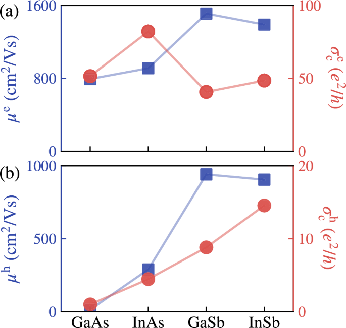
independently. In the following, _σ_c is used to denote the charge conductivity. Figure 1 presents the room temperature mobilities of the pristine monolayers and the conductivities of doped
systems. All the materials exhibit high electron mobilities, thanks to the small electron-effective mass and the single valley in the conduction bands. More variations in the hole mobility
are observed due to the multi-peak band structures. The two arsenides present different mobilities of 14 and 289 cm2/Vs, while two similar values, 940 and 904, are observed in the
antimonides. A detailed analysis of mobility mechanisms is given in another work33. In this paper, the conductivities in doped III-V monolayers are extensively explained. Doping is a
practical method to tune the transport properties of semiconductors34. Sufficient carriers are induced by heavy doping, which turns semiconductors into metallic systems where SHE can occur.
Considering the densities of states (DOS), an electron doping of 1 × 1013 cm−2 and a hole doping of 2 × 1013 cm−2 are respectively applied to the III-V monolayers, whose structures have been
relaxed again. The main impact of such doping is the shift of Fermi energy (EF) by a few hundred meV, leaving the crystal structure and electronic bands nearly unaffected as verified by
Supplementary Fig. 3. Interestingly, an electron-hole asymmetry occurs in the phonon dispersions of the III-V monolayers: the phonon dispersion is weakly affected by electron doping, while
the softening of longitudinal optical (LO) modes specifically occurs in the hole doping cases as shown in Fig. 2. The asymmetry can be explained by the difference in conduction and valence
bands. For electron doping, the Γ valley is mainly occupied, leading to a limited change compared with the conduction bands in the pristine case. In contrast, for hole doping, multiple
inequivalent peaks around Γ and K points enter into the transport window, enhancing the effective scattering \(\frac{-\partial {f}_{n{{\bf{k}}}}^{0}}{\partial {\varepsilon
}_{n{{\bf{k}}}}}{\tau }_{n{{\bf{k}}}}^{-1}\). Besides, attributed to the higher carrier concentration of 2 × 1013 cm−2 and consequent stronger screening effect, the hole doping induces a
stronger phonon softening effect, which also occurs in other hole-doped III-V monolayers, see details in Supplementary Fig. 4. In a nutshell, the asymmetry in the conduction and valence
bands leads to a limited scattering in electron-doped systems as verified by the high \({\sigma }_{{{\rm{c}}}}^{{{\rm{e}}}}\) in Fig. 1a and an enhanced scattering in hole-doped systems as
verified by the low \({\sigma }_{{{\rm{c}}}}^{{{\rm{h}}}}\) in Fig. 1b. It is expected that the charge conductivity should be proportional to the carrier mobility. However, Fig. 1a
illustrates that GaAs present a much lower _μ_e but higher \({\sigma }_{{{\rm{c}}}}^{{{\rm{e}}}}\) than GaSb with the same electron doping. In Fig. 1b, GaSb shows a high _μ_h but a low
\({\sigma }_{{{\rm{c}}}}^{{{\rm{h}}}}\) with the hole doping. These unusual behaviors are attributed to the heavy doping, which leads to a distinct transport from the intrinsic case. In
intrinsic semiconductors, the mobility is independent of _n_c. However, in heavy doping cases, semiconductors acquire a metallic character, and the mobility in doped systems depends on the
band structure as well as EF location determined by doping concentration. As a result, the linearly proportional relation between undoped mobility and heavily doped conductivity is no longer
valid. The effect on transport induced by doping will be interpreted within the self-energy relaxation time approximation32, where the conductivity is inversely proportional to the
scattering rate and directly proportional to carrier velocity. Considering the Fermi-Dirac distribution at equilibrium and 300 K, we define the K-resolved scattering rates as
\({\tau}_{{{\bf{k}}}}^{-1}={\sum}_{n}\frac{-\partial {f}_{n\bf{k}}^{0}}{\partial {\varepsilon }_{n{{\bf{k}}}}}{\tau }_{n{{\bf{k}}}}^{-1}\), and K-resolved velocities as _v_K = ∑_n__v__n_K,
where _n_ denotes the number of bands involved in the transport. Figure 3 compares the electronic structures, \({\tau }_{{{\bf{k}}}}^{-1}\), and _v_K of doped GaAs and GaSb. The
broken-inversion symmetry in pristine GaAs and GaSb monolayers results in a Rashba splitting35 in the conduction band minimum (CBM) which can be regarded as a single valley. After electron
doping, Fig. 3a shows that for GaAs, the single valley is preserved in the Fermi surface window [EF − 0.3 eV, EF + 0.3 eV], while Fig. 3d shows that for GaSb, more states around M and K
points enter into the window, leading to enhanced scatterings with states that possess low velocities. As a result, \({\sigma }_{{{\rm{c}}}}^{{{\rm{e}}}}\) in GaSb is reduced, as shown in
Fig. 1a. The surprising behaviors of _μ_h and \({\sigma }_{{{\rm{c}}}}^{{{\rm{h}}}}\) of GaSb in Fig. 1b can be attributed to the doping-induced EF shift. The valence band maximum (VBM) of
pristine GaAs locates at K points, leading to a multi-peak band structure and a high DOS around VBM, thus the hole doping can only induce a small EF shift, as shown in Fig. 3g. Besides, the
spin-orbit splitting at K in the electronic band is 12 meV, which matches well with the phonon energy at K in the phonon dispersion [see Fig. 2c]. Considering momentum and energy
conservations, the strong inter-peak scatterings between the K and K’ peaks are allowed in hole-doped GaAs. Differently, the VBM in pristine GaSb is located at Γ, which is a single peak for
the hole mobility and leads to a high _μ_h. The single-peak band structure gives a small DOS around VBM, thus a large EF shift of 0.21 eV is induced by the hole doping as shown in Fig. 3j,
leading the states around K to dominate the scattering. Considering the low velocities at K points, \({\sigma }_{{{\rm{c}}}}^{{{\rm{h}}}}\) is greatly reduced compared with _μ_h in GaSb. It
should be noted that for GaSb, the spin-orbit splitting at K is 40 meV, mismatching the phonon energy [see Fig. 2f], thus the inter-peak scattering between K and K’ is weakened compared with
GaAs, as shown by the colors in Fig. 3h and k. The discussions above demonstrate that doping is an effective way to manipulate the electronic structure, further controlling the EPI and
charge conductivity in semiconductors. Analyses of scatterings in other III-V monolayers are similar, as given in Supplementary Fig. 5. SPIN HALL CONDUCTIVITY SHE is composed of intrinsic
and extrinsic contributions. The former is defined by the Kubo formula, and the latter is due to the skew-scattering and side-jump mechanisms, strongly dependent on disorder36,37,38. In this
work, we focus on the intrinsic SHC in a weak scattering limit. With spin current along _x_, electric field along _y_, and spin orientation along _z_ direction, the intrinsic SHC is
calculated using Kubo formula39,40: $${\sigma }_{{{\rm{s}}}}=\frac{\hslash }{2e}\frac{{e}^{2}}{\hslash }{\int}_{{{\rm{BZ}}}}\frac{{{{\rm{d}}}}^{2}{{\bf{k}}}}{{(2\pi)}^{2}}{\Omega
}_{{{\rm{s}}}}({{\bf{k}}}),$$ (4) where Ωs(K) = ∑_n__f__n_KΩs,_n_(K) is the spin Berry curvature (SBC) with _f__n_K at 300 K and the band-resolved SBC as $${\Omega
}_{{{\rm{s}}},n}({{\bf{k}}})={\hslash }^{2}\mathop{\sum}\limits_{m\ne n}\frac{-2\,{{\rm{Im}}}[\left\langle n{{\bf{k}}}\right\vert {\hat{j}}_{z}\left\vert m{{\bf{k}}}\right\rangle
\left\langle m{{\bf{k}}}\right\vert {\hat{v}}_{y}\left\vert n{{\bf{k}}}\right\rangle ]}{{({\varepsilon }_{n{{\bf{k}}}}-{\varepsilon }_{m{{\bf{k}}}})}^{2}+{\eta }^{2}},$$ (5) where
\({\hat{j}}_{z}=\frac{1}{2}\{{\hat{\sigma }}_{z}{\hat{v}}_{x}+{\hat{v}}_{x}{\hat{\sigma }}_{z}\}\) is the spin current operator, \({\hat{\sigma }}_{z}\) is the Pauli operator,
\({\hat{v}}_{x}\) and \({\hat{v}}_{y}\) are velocity operators. Considering the SOC strength in all the materials, a broadening of _η_ = 2 meV is used as a weak scattering induced by
extrinsic factors41, and the _η_ value has been validated in Supplementary Fig. 6. Due to the low conductivities, the hole-doped systems are more promising for high SHRs, thus III-V
monolayer with 2 × 1013 cm−2 hole doping are targeted for SHCs, and this doping level has been realized in 2D systems42,43. Figure 4a presents the energy-dependent SHCs of hole-doped
materials at room temperature. GaAs exhibits \({\sigma }_{{{\rm{s}}}}^{{{\rm{h}}}}=0.6\) (_ℏ_/2_e_)_e_2/_h_ due to the small EF shift induced by doping. More prominently, SHCs of InAs, GaSb,
and InSb can reach up to 1.5, 2.0, and 1.8 (_ℏ_/2_e_)_e_2/_h_, respectively. For comparison, MoS2 monolayer only reaches \({\sigma }_{{{\rm{s}}}}^{{{\rm{h}}}}\approx 0.2\)
(_ℏ_/2_e_)_e_2/_h_ 22. The high SHCs in hole-doped III-V monolayers are attributed to the in-gap EF location, as shown in Fig. 3j. The spin-orbit gap separates the positive and negative SBC.
When the EF locates inside the spin-orbit gap, SHC, as the integration over the Fermi sea of SBC, can be maximized by the sign-invariant SBC over all the K-points. The SBC decompositions of
all the materials are presented in Supplementary Fig. 8. For GaAs, the SBC originates from both K and Γ points, while for the others, the SBC mainly stems from the Γ point due to the in-gap
EF at Γ. The discussions above highlight that the doping in semiconductors can yield large SHCs in III-V monolayers. SPIN HALL RATIO With the charge conductivities _σ_c and spin Hall
conductivities _σ_s, the spin Hall ratio \(\xi =\frac{2e}{\hslash }\left\vert \right.\frac{{\sigma }_{{{\rm{s}}}}}{{\sigma }_{{{\rm{c}}}}}\left\vert \right.\) can be discussed in hole-doped
systems. It has been illustrated in Supplementary Table 1 that the computational and experimental SHR values coincide with each other, i.e., both present _ξ_ ~ 0.01 in heavy metals,
demonstrating the effectiveness of our calculations. Figure 4b shows that large \({\sigma }_{{{\rm{s}}}}^{{{\rm{h}}}}\) values are found in antimonides which also possess fairly large
\({\sigma }_{{{\rm{c}}}}^{{{\rm{h}}}}\), as a result, GaSb and InSb exhibit _ξ_h = 0.23 and 0.13, respectively. More importantly, hole-doped arsenides are perfect candidates with high SHCs
and low charge transports, yielding exceptional _ξ_h = 0.58 and 0.34 in GaAs and InAs, respectively. Compared with heavy metals where _ξ_ ~ 0.01, the hole-doped GaAs and other III-V
monolayers exhibit great potential for efficient charge-to-spin conversion. SPIN HALL RATIO DESCRIPTOR Taking the transport behaviors in III-V monolayers as a prototype, a descriptor to
enhance SHR can be proposed. The idea is to decrease the charge conductivity as well as increase SHC. Large effective mass reduces _σ_c via lowering down the carrier velocity. As shown in
Fig. 3, the band structure with multiple extrema around EF can enhance scattering. Besides, the energy-dependent SHCs demonstrate that SHC can be maximized by locating EF in the spin-orbit
gap. Overall, a band structure descriptor for high SHR can be proposed as depicted in Fig. 5: (1) large effective mass \({m}_{{{\rm{K}}}}^{* }\) around EF ; (2) multiple K-inequivalent
extrema around EF ; (3) a EF located inside the spin-orbit splitting \(\Delta {\varepsilon }_{{{\rm{K}}}}^{mn}\). It should be stressed that within a limited doping concentration, there is a
competition between the first two conditions and the last one, since flat and multiple band extrema would induce a large DOS, which hinders the tuning of EF. A small effective mass at Γ
point, \({m}_{\Gamma }^{* }\), is also preferred for tuning EF when _ε_Γ > _ε_K. In short, a delicate balance between _σ_c and _σ_s is essential for SHR enhancement. HIGH-THROUGHPUT
CALCULATIONS Potential candidates for high SHR can be found by screening a database with the aforementioned descriptor. Focusing on the 2D materials, we perform fully relativistic
high-throughput calculations for exfoliable monolayers. From the MC2D database44,45, all the rare-earth free materials with up to 6 atoms per unit cell are considered, yielding 216
semiconductors which are employed for the fully relativistic DFT calculations and Wannierizations. The band interpolation quality of Wannier Hamiltonian is measured by the average band
distance, given as46,47 $${\eta }_{\nu }=\sqrt{\frac{{\sum }_{n{{\bf{k}}}}{\tilde{f}}_{n{{\bf{k}}}}{\left({\varepsilon }_{n{{\bf{k}}}}^{{{\rm{DFT}}}}-{\varepsilon
}_{n{{\bf{k}}}}^{{{\rm{Wan}}}}\right)}^{2}}{{\sum }_{n{{\bf{k}}}}{\tilde{f}}_{n{{\bf{k}}}}}}$$ (6) where K is the eigenstate along the high-symmetry K-path for band structure,
\({\tilde{f}}_{n{{\bf{k}}}}=\sqrt{{f}_{n{{\bf{k}}}}^{{{\rm{DFT}}}}\left({{{\rm{E}}}}_{{{\rm{F}}}}+\nu ,\sigma \right){f}_{n{{\bf{k}}}}^{{{\rm{Wan}}}}\left({{{\rm{E}}}}_{{{\rm{F}}}}+\nu
,\sigma \right)}\) where \(f\left({{{\rm{E}}}}_{{{\rm{F}}}}+\nu ,\sigma \right)\) is the Fermi-Dirac distribution. Here EF + _ν_ and _σ_ respectively represent energy position and smearing
value for the distribution, thus we can focus on the bands below EF + _ν_ in energy. EF is set as the CBM of semiconductor, and _σ_ is fixed to be 300 K. Since the Wannier Hamiltonian
describes the low-energy valence electrons, it is expected that the Wannier-interpolated band will deviate more from the DFT results in the higher conduction band region. Therefore, the
higher _ν_ is, the larger _η__ν_ is expected to be. The symbols _η_1 and _η_2 denote the band distance for the bands below EF + 1 eV and EF + 2 eV, respectively, and the band distances of
216 materials are present in Fig. 6. For the bands below EF + 1 eV, 97% (210/216) of materials show a small band distance below 10 meV, and 93% (200/216) of materials show a very small band
distance below 2 meV. For the bands below EF + 2 eV, 90% (195/216) of materials show a distance below 10 meV, and 65% (141/216) of materials show a distance below 2 meV, highlighting the
overall quality of Wannier Hamiltonians in our database. Figure 7 shows the electron and hole effective masses of all the semiconductors, as well as SHC values in the doped systems where a
doping concentration of 2 × 1013 cm−2 is employed for both carriers. The effective mass is calculated by \({m}_{\alpha \alpha }^{* }={(\frac{1}{{\hslash }^{2}}\frac{{d}^{2}\varepsilon
}{d{k}_{\alpha }^{2}})^{-1}}\) (_α_ = _x_, _y_) through the interpolation around CBM and VBM, respectively, for electron and hole. Overall, the hole presents a larger effective mass than the
electron, and hole-doped materials exhibit larger SHC values. Nevertheless, many materials with high SHCs present small effective masses, populated at the left lower corner in Fig. 7b.
Still, by setting the screening conditions as \({m}_{xx}^{* }\approx {m}_{yy}^{* } > 0.5\,{m}_{0}\), multiple band extrema around EF, and SHC >0.4 (_ℏ_/2_e_)_e_2/_h_, two MXene
monolayers are selected as candidates, Sc2CCl2 and Y2CBr2. All the effective masses, doped SHCs, energy gaps, and band structures of all the 216 semiconductors are reported in Supplementary
Table 5 and its followings. RESULTS OF MXENE MONOLAYERS Sc2CCl2 and Y2CBr2 present similarities since they are composed of homologous elements. After a full relaxation considering the hole
doping, both structures present a P-3m1 space group, as shown in Fig. 8d. Figure 8a and e illustrate the hole-doped band structures of Sc2CCl2 and Y2CBr2, respectively. The SOC splitting
induces two peaks around Γ point, and the top band presents an effective mass \({m}_{xx}^{* }={m}_{yy}^{* }\approx 0.7\,{m}_{0}\). EF locates inside the gap, leading to high \({\sigma
}_{{{\rm{s}}}}^{{{\rm{h}}}}\) = 0.5 (_ℏ_/2_e_)_e_2/_h_. It has been verified that SHCs in both materials are robust against broadening, and the main SBC contributions originate from the Γ
point, details are given in Supplementary Fig. 12. Compared with Y2CBr2 possessing an SOC gap of 75 meV at Γ, Sc2CCl2 shows a smaller gap of 20 meV due to lighter elements. Apart from the Γ
point, eigenstates around the M point also enter into the Fermi surface window. Figure 8b, f validate the mechanical stabilities of hole-doped Sc2CCl2 and Y2CBr2 monolayers by showing phonon
dispersions without imaginary frequency. Phonon dispersions illustrate that Sc2CCl2 presents higher-energy modes than Y2CBr2. Figure 8c and g show the K-resolved scattering rates of both
materials. Sc2CCl2 exhibits dominant scattering as high as 836 THz around the Γ point. This high rate is attributed to its small SOC gap of 20 meV which matches the phonon energy _ω__n_Γ. On
the other hand, the scattering in Y2CBr2 is limited to 370 THz, since its large gap of 75 meV goes beyond its phonon energy range. Compared with the Γ point, scatterings around M points are
quite weak. This is attributed to _ε_M = − 273 meV for Sc2CCl2 and −57 meV for Y2CBr2, thus the scattering contributions are greatly limited by the large distance from EF. Overall, Sc2CCl2
presents lower \({\sigma }_{{{\rm{c}}}}^{{{\rm{h}}}}\) = 2.2 _e_2/_h_ while Y2CBr2 shows \({\sigma }_{{{\rm{c}}}}^{{{\rm{h}}}}\) = 3.9 _e_2/_h_ in Fig. 8h. Benefiting from the low charge
conductivity, the SHR in Sc2CCl2 is computed to be _ξ_h = 0.22, and Y2CBr2 possesses _ξ_h = 0.12. The discovery of an MXene monolayer with high SHR validates the effectiveness of the SHR
descriptor. Discussions of III-V monolayers and MXene monolayers indicate that compared with the materials composed of heavy elements, the light materials can be more promising for high SHR.
Although the heavy elements induce strong SOC for SHC enhancement, they also result in large band splitting and low-energy phonon mode simultaneously. By breaking the energy conservation
rule, these two factors reduce the electron-phonon coupling and hinder the scatterings in charge transport. As a result, the charge conductivity is also enhanced. Since the charge-to-spin
conversion is an interrelated process, balancing charge and spin transports is critical to enhance SHR rather than only maximize SHC. In addition, compared with the SHR _ξ_h = 0.58 in GaAs,
_ξ_h = 0.22 in Sc2CCl2 is relatively lower. Considering that the SHC values in the two materials are similar, the SHR difference is attributed to the high \({\sigma
}_{{{\rm{c}}}}^{{{\rm{h}}}}\) in Sc2CCl2. In GaAs, strong inter-peak scatterings occur [see Fig. 3h] thanks to the K eigenstates around EF. In contrast, Sc2CCl2 exhibits weak scatterings
around the M point [see Fig. 8c] due to the M eigenstates far away from EF. Besides, the inversion symmetry keeps the band degeneracy in Sc2CCl2, further reducing the scattering
possibilities. This comparison demonstrates the importance of multi-peaks around EF to reduce charge conductivity, further validating the SHR descriptor. By expanding the high-throughput
calculations database, materials with more ideal electronic structures and phonon frequencies could be found for SHR enhancement. EXPERIMENTAL FEASIBILITY Charge-to-spin conversion has been
realized in MoS2 and WSe2 monolayers grown by chemical vapor deposition19. Since the first synthesis of 2D AlN layers by metal organic deposition48, many efforts have been devoted to the
synthesis of other 2D III-V materials49,50. For example, GaSb films can be grown via a seeded lateral epitaxy, and the free-standing crystalline GaSb can be exfoliated from these films51.
Moreover, 2D InAs flakes with high crystalline quality have been synthesized through van der Waals epitaxy with a thickness down to 4.8 nm52. Due to chemical similarity in one family, we
expect similar techniques can be applied to the other III-V monolayers. Two promising materials, Sc2CCl2 and Y2CBr2, are easily exfoliable from their van der Waals bulk compounds45. Finally,
the doping levels proposed in this work can be realized via the advanced technique of electron beam, which implements the doping of 1.7 × 1013 cm−2 in 2D systems42. The doped state persists
even after removing the electron beam and back-gate voltage, and the process is reversible and repeatable42. Moreover, the doping level over 5 × 1013 cm−2 has been realized in MoS2
monolayers via the ionic-liquid gate43. In conclusion, 2D materials with high spin Hall ratios have been found using a multidisciplinary investigation involving charge transport, spin Hall
conductivity, and a high-throughput database. The hole-doped GaAs monolayer presents an ultrahigh SHR of _ξ_ = 0.58, attributed to the strong scattering and the high SHC. An SHR descriptor
is proposed and validated by a high-throughput database of 216 exfoliable monolayer semiconductors, suggesting a new promising material, Sc2CCl2. Besides, this database is fully released to
the community. This work reveals potential 2D materials for efficient charge-to-spin conversion, providing a guideline for materials discovery in spintronics. METHODS DFT CALCULATIONS DFT
and DFPT calculations are performed by the Quantum ESPRESSO package53. The fully relativistic norm-conserving pseudopotentials PseudoDojo54 within the Perdew–Burke–Ernzerhof (PBE)
parametrization of the generalized gradient approximation (GGA)54. The cutoff energy for wavefunctions is set to 120 Ry. We use a 2D Coulomb truncation55. Fully relativistic computations
have been performed for structural relaxation, self-consistent, non-self-consistent, and phonon calculations. Relaxations are performed respectively for pristine and doped materials.
Variable cell relaxation is performed with total energy convergence of 10−8 Ry, force convergence of 10−4 Ry/Bohr, and pressure convergence of 0.1 kbar. CHARGE CONDUCTIVITY CALCULATIONS The
drift mobility and charge conductivity are calculated using the EPW package56,57, where the electron-phonon coupling is interpolated from coarse K/Q-grids to fine K/Q-grids using Wannier
functions with the considerations of dipole, quadrupole, and gauge-covariant contributions58,59. A coarse 12 × 12 × 1 K/Q-grid is adopted in ab initio calculations, then a fine K/Q-grid of
720 × 720 × 1 is used for electron mobility, and K/Q-grid of 360 × 360 × 1 for hole mobility and charge conductivity of doped systems. Note that in the calculation at the zone-center Q = Γ,
a denser K-grid of 32 × 32 × 1 is used in DFPT calculation to get convergent electrostatic properties. A Fermi surface window of 0.3 eV has been validated for convergence and employed in all
calculations. An adaptive smearing60 is applied in the energy-conserving delta functions, and a phonon frequency cutoff of 1 cm−1 is employed. The calculations are performed at room
temperature. SPIN HALL CONDUCTIVITY CALCULATIONS The spin Hall conductivity is calculated by Wannier90 package39,61, with a 12 × 12 × 1 coarse K-grid in ab initio calculation, and a fine
K-grid of 360 × 360 × 1 for the Wannier interpolation. A Fermi-Dirac distribution function of 300 K and a broadening of 2 meV have been considered. HIGH-THROUGHPUT CALCULATIONS The fully
relativistic DFT calculations and Wannierizations have been performed using AiiDA62 and PseudoDojo54 on 216 materials from the MC2D database44,45. The initial guess for projectors is given
by the orbital information in PseudoDojo63. The semicore orbitals corresponding to deep bands are excluded from projections. A small trial step is used in the minimization of the spread
function to stabilize the Wannierization, and a large number of iterations is used to converge. The maximum of the frozen window is set as CBM + 2 eV, which is verified to be the optimal
value by Supplementary Fig. 13. The script for the automated generation of the Wannier90 input file is provided64. To provide a high-quality Wannier Hamiltonian database, failed cases
(23/216) have been manually corrected by tuning the frozen window, increasing the number of Bloch wavefunctions, or manually modifying initial projections. DATA AVAILABILITY For the III-V
and MXene monolayers investigated in this work, details of the relaxed atomic structures, effective masses, densities of states, doping levels, and electron and phonon dispersions are given
in Supplementary Material, and input and output files for computations are given on Materials Cloud Archive64. The input and output files, pseudopotentials, as well as Wannier Hamiltonians
and band structures of 216 monolayer semiconductors, are provided on Materials Cloud Archive64. REFERENCES * Inoue, J. & Ohno, H. Taking the Hall effect for a spin. _Science_ 309, 2004
(2005). Article CAS PubMed Google Scholar * Chang, C.-Z. & Li, M. Quantum anomalous Hall effect in time-reversal-symmetry breaking topological insulators. _J. Phys. Condens. Matter_
28, 123002 (2016). Article PubMed Google Scholar * Ashcroft,N., W. & Mermin, N. D. _Solid State Physics_ (Hartcourt College publisher, 1976) * Sinova, J., Valenzuela, S. O.,
Wunderlich, J., Back, C. H. & Jungwirth, T. Spin Hall effects. _Rev. Mod. Phys._ 87, 1213 (2015). Article Google Scholar * Manchon, A. et al. Current-induced spin-orbit torques in
ferromagnetic and antiferromagnetic systems. _Rev. Mod. Phys._ 91, 035004 (2019). Article CAS Google Scholar * Guo, Z. et al. Spintronics for energy- efficient computing: an overview and
outlook. _Proc. IEEE_ 109, 1398 (2021). Article CAS Google Scholar * Žutić, I., Fabian, J. & Das Sarma, S. Spintronics: fundamentals and applications. _Rev. Mod. Phys._ 76, 323
(2004). Article Google Scholar * Olejník, K. et al. Detection of electrically modulated inverse spin hall effect in an Fe/GaAs microdevice. _Phys. Rev. Lett._ 109, 076601 (2012). Article
PubMed Google Scholar * Tao, X. et al. Self-consistent determination of spin Hall angle and spin diffusion length in Pt and Pd: the role of the interface spin loss. _Sci. Adv._ 4, eaat1670
(2018). Article PubMed PubMed Central Google Scholar * Dc, M. et al. Room-temperature high spin-orbit torque due to quantum confinement in sputtered Bi_x_Se1−_x_ films. _Nat. Mater._
17, 800 (2018). Article CAS PubMed Google Scholar * Khang, N. H. D., Ueda, Y. & Hai, P. N. A conductive topological insulator with large spin Hall effect for ultralow power
spin-orbit torque switching. _Nat. Mater._ 17, 808 (2018). Article CAS PubMed Google Scholar * Zhou, J., Qiao, J., Bournel, A. & Zhao, W. Intrinsic spin Hall conductivity of the
semimetals MoTe2 and WTe2. _Phys. Rev. B_ 99, 060408(R) (2019). Article Google Scholar * Zhao, B. et al. Observation of charge to spin conversion in Weyl semimetal WTe2 at room
temperature. _Phys. Rev. Res._ 2, 013286 (2020). Article CAS Google Scholar * Vila, M. et al. Low-symmetry topological materials for large charge-to-spin interconversion: the case of
transition metal dichalcogenide monolayers. _Phys. Rev. Res._ 3, 043230 (2021). Article CAS Google Scholar * Song, P. et al. Coexistence of large conventional and planar spin Hall effect
with long spin diffusion length in a low-symmetry semimetal at room temperature. _Nat. Mater._ 19, 292 (2020). Article CAS PubMed Google Scholar * Marrazzo, A., Gibertini, M., Campi, D.,
Mounet, N. & Marzari, N. Relative abundance of Z2 topological order in exfoliable two-dimensional insulators. _Nano Lett._ 19, 8431 (2019). Article CAS PubMed Google Scholar *
Grassano, D., Marzari, N. & Campi, D. High-throughput screening of Weyl semimetals. _Phys. Rev. Mater._ 8, 024201 (2024). Article CAS Google Scholar * Dorow, C. et al. Advancing
monolayer 2-d nmos and pmos transistor integration from growth to van der waals interface engineering for ultimate cmos scaling. _IEEE Trans. Electron Dev._ 68, 6592 (2021). Article CAS
Google Scholar * Shao, Q. et al. Strong Rashba-Edelstein effect-induced spin-orbit torques in monolayer transition metal dichalcogenide/ferromagnet bilayers. _Nano Lett._ 16, 7514 (2016).
Article CAS PubMed Google Scholar * Wang, H. et al. Interfacial engineering of ferromagnetism in wafer-scale van der Waals Fe4GeTe2 far above room temperature. _Nat. Commun._ 14, 1
(2023). Google Scholar * Wang, H. et al. Room temperature energy-efficient spin-orbit torque switching in two-dimensional van der Waals Fe3GeTe2 induced by topological insulators. _Nat.
Commun._ 14, 1 (2023). Google Scholar * Feng, W. et al. Intrinsic spin Hall effect in monolayers of group-VI dichalcogenides: a first-principles study. _Phys. Rev. B_ 86, 165108 (2012).
Article Google Scholar * Sohier, T., Campi, D., Marzari, N. & Gibertini, M. Mobility of two-dimensional materials from first principles in an accurate and automated framework. _Phys.
Rev. Mater._ 2, 114010 (2018). Article CAS Google Scholar * Wang, H. et al. Spin Hall effect in prototype Rashba ferroelectrics GeTe and SnTe. _npj Comput. Mater._ 6, 1 (2020). Article
Google Scholar * Backman, J., Lee, Y. & Luisier, M. Electron-phonon calculations using a Wannier-based supercell approach: applications to the monolayer MoS2 mobility. _Solid State
Electron._ 198, 108461 (2022). Article CAS Google Scholar * Zhang, C., Wang, R., Mishra, H. & Liu, Y. Two-dimensional semiconductors with high intrinsic carrier mobility at room
temperature. _Phys. Rev. Lett._ 130, 087001 (2023). Article CAS PubMed Google Scholar * Cepellotti, A., Coulter, J., Johansson, A., Fedorova, N. S. & Kozinsky, B. Phoebe: a
high-performance framework for solving phonon and electron Boltzmann transport equations. _J. Phys. Mater._ 5, 035003 (2022). Article CAS Google Scholar * Giustino, F. Electron-phonon
interactions from first principles. _Rev. Mod. Phys._ 89, 015003 (2017). Article Google Scholar * Kohn, W. Nobel lecture: electronic structure of matter—wave functions and density
functionals. _Rev. Mod. Phys._ 71, 1253 (1999). Article CAS Google Scholar * Baroni, S., de Gironcoli, S., Dal Corso, A. & Giannozzi, P. Phonons and related crystal properties from
density-functional perturbation theory. _Rev. Mod. Phys._ 73, 515 (2001). Article CAS Google Scholar * Marzari, N., Mostofi, A. A., Yates, J. R., Souza, I. & Vanderbilt, D. Maximally
localized Wannier functions: theory and applications. _Rev. Mod. Phys._ 84, 1419 (2012). Article CAS Google Scholar * Poncé, S., Li, W., Reichardt, S. & Giustino, F. First-principles
calculations of charge carrier mobility and conductivity in bulk semiconductors and two-dimensional materials. _Rep. Prog. Phys._ 83, 036501 (2020). Article PubMed Google Scholar * Zhou,
J., Poncé, S. & Charlier, J.-C. Guidelines for accurate and efficient calculations of mobilities in two-dimensional materials. _Phys. Rev. B_ 110, 125304 (2024). Article Google Scholar
* Awate, S. S. et al. Impact of large gate voltages and ultrathin polymer electrolytes on carrier density in electric-double-layer-gated two-dimensional crystal transistors. _ACS Appl.
Mater. Interfaces_ 15, 15785 (2023). Article CAS PubMed PubMed Central Google Scholar * Wu, K. et al. Two-dimensional giant tunable Rashba semiconductors with two-atom-thick buckled
honeycomb structure. _Nano Lett._ 21, 740 (2021). Article CAS PubMed Google Scholar * Lowitzer, S. et al. Extrinsic and intrinsic contributions to the spin Hall effect of alloys. _Phys.
Rev. Lett._ 106, 056601 (2011). Article PubMed Google Scholar * Gorini, C., Eckern, U. & Raimondi, R. Spin Hall effects due to phonon skew scattering. _Phys. Rev. Lett._ 115, 076602
(2015). Article PubMed Google Scholar * Shashank, U. et al. Disentanglement of intrinsic and extrinsic side-jump scattering induced spin Hall effect in N-implanted Pt. _Phys. Rev. B_ 107,
064402 (2023). Article CAS Google Scholar * Qiao, J., Zhou, J., Yuan, Z. & Zhao, W. Calculation of intrinsic spin Hall conductivity by Wannier interpolation. _Phys. Rev. B_ 98,
214402 (2018). Article CAS Google Scholar * Zhang, Y. et al. Different types of spin currents in the comprehensive materials database of nonmagnetic spin Hall effect. _npj Comput. Mater._
7, 1 (2021). Google Scholar * Li, H. et al. Intraband and interband spin-orbit torques in noncentrosymmetric ferromagnets. _Phys. Rev. B_ 91, 134402 (2015). Article Google Scholar * Shi,
W. et al. High-order fractal quantum oscillations in graphene/BN superlattices in the extreme doping limit. _Phys. Rev. Lett._ 130, 186204 (2023). Article CAS PubMed Google Scholar *
Sohier, T. et al. Enhanced electron-phonon interaction in multivalley materials. _Phys. Rev. X_ 9, 031019 (2019). CAS Google Scholar * Mounet, N. et al. Two-dimensional materials from
high-throughput computational exfoliation of experimentally known compounds. _Nat. Nanotechnol._ 13, 246 (2018). Article CAS PubMed Google Scholar * Campi, D., Mounet, N., Gibertini, M.,
Pizzi, G. & Marzari, N. Expansion of the materials cloud 2D database. _ACS Nano_ 17, 11268 (2023). Article CAS PubMed PubMed Central Google Scholar * Qiao, J., Pizzi, G. &
Marzari, N. Automated mixing of maximally localized Wannier functions into target manifolds. _npj Comput. Mater._ 9, 1 (2023). Article Google Scholar * Qiao, J., Pizzi, G. & Marzari,
N. Projectability disentanglement for accurate and automated electronic-structure Hamiltonians. _npj Comput. Mater._ 9, 1 (2023). Article Google Scholar * Wang, W. et al. 2D AlN layers
sandwiched between graphene and Si substrates. _Adv. Mater._ 31, 1803448 (2019). Article Google Scholar * Lu, F., Wang, H., Zeng, M. & Fu, L. Infinite possibilities of ultrathin III-V
semiconductors: starting from synthesis. _iScience_ 25, 103835 (2022). Article CAS PubMed PubMed Central Google Scholar * Nikolaevich Klochkov, A. et al. Growth by molecular beam
epitaxy and characterization of n-InAs films on sapphire substrates. _Appl. Surf. Sci._ 619, 156722 (2023). Article CAS Google Scholar * Manzo, S. et al. Pinhole-seeded lateral epitaxy
and exfoliation of GaSb films on graphene-terminated surfaces. _Nat. Commun._ 13, 1 (2022). Article Google Scholar * Dai, J. et al. Controlled growth of two-dimensional InAs single
crystals via van der Waals epitaxy. _Nano Res._ 15, 9954 (2022). Article CAS Google Scholar * Giannozzi, P. et al. Advanced capabilities for materials modelling with Quantum ESPRESSO. _J.
Phys. Condens. Matter_ 29, 465901 (2017). Article CAS PubMed Google Scholar * van Setten, M. J. et al. The PseudoDojo: training and grading a 85 element optimized norm-conserving
pseudopotential table. _Comput. Phys. Commun._ 226, 39 (2018). Article Google Scholar * Sohier, T., Calandra, M. & Mauri, F. Density functional perturbation theory for gated
two-dimensional heterostructures: theoretical developments and application to flexural phonons in graphene. _Phys. Rev. B_ 96, 075448 (2017). Article Google Scholar * Poncé, S., Margine,
E., Verdi, C. & Giustino, F. EPW: electron-phonon coupling, transport and superconducting properties using maximally localized wannier functions. _Comput. Phys. Commun._ 209, 116 (2016).
Article Google Scholar * Lee, H. et al. Electron–phonon physics from first principles using the EPW code. _npj Comput. Mater._ 9, 1 (2023). Article Google Scholar * Poncé, S., Royo, M.,
Stengel, M., Marzari, N. & Gibertini, M. Long-range electrostatic contribution to electron-phonon couplings and mobilities of two-dimensional and bulk materials. _Phys. Rev. B_ 107,
155424 (2023). Article Google Scholar * Poncé, S., Royo, M., Gibertini, M., Marzari, N. & Stengel, M. Accurate prediction of Hall mobilities in two-dimensional materials through
gauge-covariant quadrupolar contributions. _Phys. Rev. Lett._ 130, 166301 (2023). Article PubMed Google Scholar * Poncé, S. et al. First-principles predictions of Hall and drift
mobilities in semiconductors. _Phys. Rev. Res._ 3, 043022 (2021). Article Google Scholar * Pizzi, G. et al. Wannier90 as a community code: new features and applications. _J. Phys. Condens.
Matter_ 32, 165902 (2020). Article CAS PubMed Google Scholar * Huber, S. P. et al. AiiDA 1.0, a scalable computational infrastructure for automated reproducible workflows and data
provenance. _Sci. Data_ 7, 1 (2020). Article Google Scholar * Pseudodojo semicore states.
https://github.com/aiidateam/aiida-wannier90-workflows/blob/main/src/aiida_wannier90_workflows/utils/pseudo/data/semicore/PseudoDojo_0.4_PBE_FR_standard_upf.json Github (2023). * Materials
Cloud Archive. https://archive.materialscloud.org/deposit/records/2138 (2024). Download references ACKNOWLEDGEMENTS The authors would like to thank Xi Dai, Matteo Giantomassi, and Junfeng
Qiao for fruitful discussions. S.P. acknowledges the support from the Fonds de la Recherche Scientifique de Belgique (F.R.S.-FNRS). J.Z. and J.-C.C. acknowledge financial support from the
Fédération Wallonie-Bruxelles through the ARC Grant “DREAMS” (No. 21/26-116), from the EOS project “CONNECT” (No. 40007563), and from the Belgium F.R.S.-FNRS through the research project
(No. T.029.22F). Computational resources have been provided by the PRACE award granting access to MareNostrum4 at Barcelona Supercomputing Center (BSC), Spain and Discoverer in SofiaTech,
Bulgaria (OptoSpin project ID. 2020225411), and by the Consortium des Équipements de Calcul Intensif (CÉCI), funded by the F.R.S.-FNRS under Grant No. 2.5020.11 and by the Walloon Region, as
well as computational resources awarded on the Belgian share of the EuroHPC LUMI supercomputer. AUTHOR INFORMATION AUTHORS AND AFFILIATIONS * Institute of Condensed Matter and Nanosciences
(IMCN), Université catholique de Louvain (UCLouvain), Chemin des Étoiles 8, B-1348, Louvain-la-Neuve, Belgium Jiaqi Zhou & Jean-Christophe Charlier * European Theoretical Spectroscopy
Facility and Institute of Condensed Matter and Nanosciences (IMCN), Université catholique de Louvain (UCLouvain), Chemin des Étoiles 8, B-1348, Louvain-la-Neuve, Belgium Samuel Poncé * WEL
Research Institute, Avenue Pasteur 6, B-1300, Wavre, Belgium Samuel Poncé Authors * Jiaqi Zhou View author publications You can also search for this author inPubMed Google Scholar * Samuel
Poncé View author publications You can also search for this author inPubMed Google Scholar * Jean-Christophe Charlier View author publications You can also search for this author inPubMed
Google Scholar CONTRIBUTIONS J.Z. designed the study and performed calculations. S.P. and J.-C.C. supervised the project. All authors analyzed the results and contributed to writing the
paper. CORRESPONDING AUTHORS Correspondence to Jiaqi Zhou, Samuel Poncé or Jean-Christophe Charlier. ETHICS DECLARATIONS COMPETING INTERESTS The authors declare no competing interests.
ADDITIONAL INFORMATION PUBLISHER’S NOTE Springer Nature remains neutral with regard to jurisdictional claims in published maps and institutional affiliations. SUPPLEMENTARY INFORMATION
SUPPLEMENTARY MATERIAL RIGHTS AND PERMISSIONS OPEN ACCESS This article is licensed under a Creative Commons Attribution-NonCommercial-NoDerivatives 4.0 International License, which permits
any non-commercial use, sharing, distribution and reproduction in any medium or format, as long as you give appropriate credit to the original author(s) and the source, provide a link to the
Creative Commons licence, and indicate if you modified the licensed material. You do not have permission under this licence to share adapted material derived from this article or parts of
it. The images or other third party material in this article are included in the article’s Creative Commons licence, unless indicated otherwise in a credit line to the material. If material
is not included in the article’s Creative Commons licence and your intended use is not permitted by statutory regulation or exceeds the permitted use, you will need to obtain permission
directly from the copyright holder. To view a copy of this licence, visit http://creativecommons.org/licenses/by-nc-nd/4.0/. Reprints and permissions ABOUT THIS ARTICLE CITE THIS ARTICLE
Zhou, J., Poncé, S. & Charlier, JC. Enhanced spin Hall ratio in two-dimensional semiconductors. _npj Comput Mater_ 10, 247 (2024). https://doi.org/10.1038/s41524-024-01434-z Download
citation * Received: 20 June 2024 * Accepted: 06 October 2024 * Published: 23 October 2024 * DOI: https://doi.org/10.1038/s41524-024-01434-z SHARE THIS ARTICLE Anyone you share the following
link with will be able to read this content: Get shareable link Sorry, a shareable link is not currently available for this article. Copy to clipboard Provided by the Springer Nature
SharedIt content-sharing initiative
Trending News
Peso slips from its strong position against the us dollarThe Mexican peso weakened to as low as 17.08 to the US dollar on Tuesday morning, a depreciation of around 4.6% compared...
Ukaea secures second athena swan bronze awardNews story UKAEA SECURES SECOND ATHENA SWAN BRONZE AWARD Second Athena SWAN Bronze Award as UKAEA sets sights on a more ...
How can i make my mexican pool eco friendly?When picturing eco-friendly pools, you may envision a natural or “bio” pool, free from chemicals and beneficial to the e...
Commission to investigate guerrero gunfight that killed 15The National Human Rights Commission (CNDH) will investigate a confrontation in Guerrero this week that left 14 suspecte...
Coahuila auditor files embezzlement complaints over 639 million pesosDuring four months ending last April, the Coahuila Auditor’s Office (ASEC) filed 13 criminal complaints against a state ...
Latests News
Enhanced spin hall ratio in two-dimensional semiconductorsABSTRACT The conversion efficiency from charge current to spin current via the spin Hall effect is evaluated by the spin...
San miguel literary sala hosts online events with film stars turned authorsAlthough the pandemic forced them into an online virtual format this year, the San Miguel Literary Sala has come out of ...
Teenagers aren’t reading enough tough books – here’s why that mattersKeith Topping ne travaille pas, ne conseille pas, ne possède pas de parts, ne reçoit pas de fonds d'une organisation qui...
Behind the scenes at mexico city's day of the dead paradeWhat began because of the 2015 James Bond film _Spectre_ has now taken on a form of its own in Mexico City. Sunday’s Day...
Visible quantum plasmonics from metallic nanodimersABSTRACT We report theoretical evidence that bulk nonlinear materials weakly interacting with highly localized plasmonic...