Repeated temperature modulation epitaxy for p-type doping and light-emitting diode based on zno
Repeated temperature modulation epitaxy for p-type doping and light-emitting diode based on zno"
- Select a language for the TTS:
- UK English Female
- UK English Male
- US English Female
- US English Male
- Australian Female
- Australian Male
- Language selected: (auto detect) - EN
Play all audios:
ABSTRACT Since the successful demonstration of a blue light-emitting diode (LED)1, potential materials for making short-wavelength LEDs and diode lasers have been attracting increasing
interest as the demands for display, illumination and information storage grow2,3,4. Zinc oxide has substantial advantages including large exciton binding energy, as demonstrated by
efficient excitonic lasing on optical excitation5,6. Several groups have postulated the use of p-type ZnO doped with nitrogen, arsenic or phosphorus7,8,9,10, and even p–n junctions11,12,13.
However, the choice of dopant and growth technique remains controversial and the reliability of p-type ZnO is still under debate14. If ZnO is ever to produce long-lasting and robust devices,
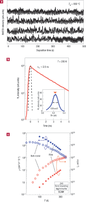
the quality of epitaxial layers has to be improved as has been the protocol in other compound semiconductors15. Here we report high-quality undoped films with electron mobility exceeding
that in the bulk. We have used a new technique to fabricate p-type ZnO reproducibly. Violet electroluminescence from homostructural p–i–n junctions is demonstrated at room-temperature.
Access through your institution Buy or subscribe This is a preview of subscription content, access via your institution ACCESS OPTIONS Access through your institution Subscribe to this
journal Receive 12 print issues and online access $259.00 per year only $21.58 per issue Learn more Buy this article * Purchase on SpringerLink * Instant access to full article PDF Buy now
Prices may be subject to local taxes which are calculated during checkout ADDITIONAL ACCESS OPTIONS: * Log in * Learn about institutional subscriptions * Read our FAQs * Contact customer
support SIMILAR CONTENT BEING VIEWED BY OTHERS LIGHT-TRIGGERED REGIONALLY CONTROLLED N-DOPING OF ORGANIC SEMICONDUCTORS Article 28 May 2025 OPERANDO ZNO RECRYSTALLIZATION FOR EFFICIENT
QUANTUM-DOT LIGHT-EMITTING DIODES Article Open access 15 May 2025 RECONFIGURABLE PHOTO-INDUCED DOPING OF TWO-DIMENSIONAL VAN DER WAALS SEMICONDUCTORS USING DIFFERENT PHOTON ENERGIES Article
14 December 2020 REFERENCES * Nakamura, S., Mukai, T. & Senoh, M. Candela-class high-brightness InGaN/AlGaN double-heterostructure blue-light emitting diodes. _Appl. Phys. Lett._ 64,
1687–1689 (1994). Article CAS Google Scholar * Kinoshita, A., Hirayama, H., Ainoya, M., Aoyagi, Y. & Hirata, A. Room-temperature operation at 333 nm of Al0.03Ga0.97N/Al0.25Ga0.75N
quantum-well light-emitting diodes with Mg-doped superlattice layers. _Appl. Phys. Lett._ 77, 175–177 (2000). Article CAS Google Scholar * Koizumi, S., Watanabe, K., Hasegawa, M. &
Kanda, H. Ultraviolet emission from a diamond pn junction. _Science_ 292, 1899–1901 (2001). Article CAS Google Scholar * Watanabe, K., Taniguchi, T. & Kanda, H. Direct-bandgap
properties and evidence for ultraviolet lasing of hexagonal boron nitride single crystal. _Nature Mater._ 3, 404–409 (2004). Article CAS Google Scholar * Bagnall, D. M. et al. Optically
pumped lasing of ZnO at room temperature. _Appl. Phys. Lett._ 70, 2230–2232 (1997). Article CAS Google Scholar * Yu, P. et al. Ultraviolet spontaneous and stimulated emissions from ZnO
microcrystalline thin films at room temperature. _Solid State Commun._ 103, 459–463 (1997). Article Google Scholar * Minegishi, K. et al. Growth of p-type zinc oxide films by chemical
vapor deposition. _Jpn J. Appl. Phys._ 36, L1453–L1455 (1997). Article CAS Google Scholar * Ryu, Y. R. et al. Synthesis of p-type ZnO films. _J. Cryst. Growth_ 216, 330–334 (2000).
Article CAS Google Scholar * Look, D. C. et al. Characterization of homoepitaxial p-type ZnO grown by molecular beam epitaxy. _Appl. Phys. Lett._ 81, 1830–1832 (2002). Article CAS
Google Scholar * Kim, K.-K., Kim, H.-S., Hwang, D.-K., Lim, J.-H. & Park, S.-J. Realization of p-type ZnO thin films via phosphorus doping and thermal activation of the dopant. _Appl.
Phys. Lett._ 83, 63–65 (2003). Article CAS Google Scholar * Aoki, T., Hatanaka, Y. & Look, D. C. ZnO diode fabricated by excimer-laser doping. _Appl. Phys. Lett._ 76, 3257–3259
(2000). Article CAS Google Scholar * Ryu, Y. R., Lee, T. S., Leem, J. H. & White, H. W. Fabrication of homostructural ZnO p-n junctions and ohmic contacts to arsenic-doped p-type ZnO.
_Appl. Phys. Lett._ 83, 4032–4034 (2003). Article CAS Google Scholar * Alivov, Y. I. et al. Fabrication and characterization of n-ZnO/p-AlGaN heterojunction light-emitting diodes on
6H-SiC substrates. _Appl. Phys. Lett._ 83, 4719–4721 (2003). Article CAS Google Scholar * Look, D. C. & Claflin, B. P-type doping and devices based on ZnO. _Phys. Status Solidi B_
241, 624–630 (2004). Article CAS Google Scholar * Haase, M. A., Qiu, J., DePuydt, J. M. & Cheng, H. Blue-green laser diodes. _Appl. Phys. Lett._ 59, 1272–1274 (1991). Article CAS
Google Scholar * Sze, S. M. _Semiconductor Devices: Physics and Technology_ Ch. 12 (Wiley, New York, 1986). Google Scholar * Chia, C. H. et al. Confinement-enhanced biexciton binding
energy in ZnO/ZnMgO multiple quantum wells. _Appl. Phys. Lett._ 82, 1848–1850 (2003). Article CAS Google Scholar * Ohtomo, A et al. Mg_x_Zn1−_x_O as a II–VI widegap semiconductor alloy.
_Appl. Phys. Lett._ 72, 2466–2468 (1998). Article CAS Google Scholar * Makino, T. et al. Band gap engineering based on Mg_x_Zn1−_x_O and Cd_y_Zn1−_y_O ternary alloy films. _Appl. Phys.
Lett._ 78, 1237–1239 (2001). Article CAS Google Scholar * Takagi, T., Tanaka, H., Fujita, S. & Fujita, S. Molecular beam epitaxy of high magnesium content single-phase wurtzite
Mg_x_Zn1−_x_O alloy (_x_ ∼ 0.5) and their application to solar-blind region photodetectors. _Jpn J. Appl. Phys._ 42, L401–L403 (2003). Article CAS Google Scholar * van de Walle, C. G.
Hydrogen as a cause of doping in zinc oxide. _Phys. Rev. Lett._ 85, 1012–1015 (2000). Article CAS Google Scholar * Theys, B. et al. Effects of intentionally introduced hydrogen on the
electrical properties of ZnO layers grown by metalorganic chemical vapor deposition. _J. Appl. Phys._ 91, 3922–3924 (2002). Article CAS Google Scholar * Tsukazaki, A. et al.
Layer-by-layer growth of high-optical-quality ZnO film on atomically smooth and lattice relaxed ZnO buffer layer. _Appl. Phys. Lett._ 83, 2784–2786 (2003). Article CAS Google Scholar *
Ohtomo, A et al. Single crystalline ZnO films grown on lattice-matched ScAlMgO4(0001) substrates. _Appl. Phys. Lett._ 75, 2635–2637 (1999). Article CAS Google Scholar * Koida, T. et al.
Correlation between the photoluminescence lifetime and defect density in bulk and epitaxial ZnO. _Appl. Phys. Lett._ 82, 532–534 (2003). Article CAS Google Scholar * Chichibu, S. F. et
al. Emission mechanisms of bulk GaN and InGaN quantum wells prepared by lateral epitaxial overgrowth. _Appl. Phys. Lett._ 74, 1460–1462 (1999). Article CAS Google Scholar * Look, D. C.,
Hemsky, J. W. & Sizelove, J. R. Residual native shallow donor in ZnO. _Phys. Rev. Lett._ 82, 2552–2555 (1999). Article CAS Google Scholar * Sumiya, M. et al. Quantitative control and
detection of heterovalent impurities in ZnO thin films grown by pulsed laser deposition. _J. Appl. Phys._ 93, 2562–2569 (2003). Article CAS Google Scholar * Ip, K. et al. Hydrogen
incorporation, diffusivity, and evolution in bulk ZnO. _Solid-State Electron._ 47, 2255–2259 (2003). Article CAS Google Scholar * Guo, X.-L., Choi, J.-H., Tabata, H. & Kawai, T.
Fabrication and optoelectronic properties of a transparent ZnO homostructural light-emitting diode. _Jpn J. Appl. Phys._ 40, L177–L180 (2001). Article CAS Google Scholar * Tsukazaki, A.
et al. Systematic examination of carrier polarity in composition spread ZnO thin films codoped with Ga and N. _Appl. Phys. Lett._ 81, 235–237 (2002). Article CAS Google Scholar * Ohnishi,
T et al. Determination of surface polarity of c-axis oriented ZnO films by coaxial impact-collision ion scattering spectroscopy. _Appl. Phys. Lett._ 72, 824–826 (1998). Article CAS Google
Scholar Download references ACKNOWLEDGEMENTS We thank T. Ohnishi and M. Lippmaa for measurement of coaxial impact-collision ion scattering spectroscopy. This work was supported by MEXT
Grant of Creative Scientific Research 14GS0204, MEXT Grant-in-Aid for Young Scientists 15685011, the Asahi Glass Foundation, and the inter-university cooperative program of the IMR. A.T. is
supported by a JSPS fellowship and S.F.C. is supported by the MEXT-COE21 program. AUTHOR INFORMATION AUTHORS AND AFFILIATIONS * Institute for Materials Research, Tohoku University, Sendai,
980-8577, Japan Atsushi Tsukazaki, Akira Ohtomo, Makoto Ohtani & Masashi Kawasaki * Institute of Applied Physics and Graduate School of Pure and Applied Sciences, University of Tsukuba,
Tsukuba, 305-8573, Japan Takeyoshi Onuma & Shigefusa F. Chichibu * Photodynamics Research Center, The Institute of Physical and Chemical Research (RIKEN), Sendai, 980-0845, Japan
Takayuki Makino, Shigefusa F. Chichibu & Yusaburou Segawa * Department of Electrical and Electronic Engineering, Shizuoka University, Hamamatsu, 432-8561, Japan Masatomo Sumiya &
Syunrou Fuke * Research Institute of Electrical Communication, Tohoku University, Sendai, 980-8577, Japan Keita Ohtani & Hideo Ohno * Materials and Structures Laboratory, Tokyo Institute
of Technology, Yokohama, 226-8503, Japan Hideomi Koinuma * Combinatorial Material Science and Technology (COMET), Tsukuba, 305-0044, Japan Hideomi Koinuma & Masashi Kawasaki Authors *
Atsushi Tsukazaki View author publications You can also search for this author inPubMed Google Scholar * Akira Ohtomo View author publications You can also search for this author inPubMed
Google Scholar * Takeyoshi Onuma View author publications You can also search for this author inPubMed Google Scholar * Makoto Ohtani View author publications You can also search for this
author inPubMed Google Scholar * Takayuki Makino View author publications You can also search for this author inPubMed Google Scholar * Masatomo Sumiya View author publications You can also
search for this author inPubMed Google Scholar * Keita Ohtani View author publications You can also search for this author inPubMed Google Scholar * Shigefusa F. Chichibu View author
publications You can also search for this author inPubMed Google Scholar * Syunrou Fuke View author publications You can also search for this author inPubMed Google Scholar * Yusaburou
Segawa View author publications You can also search for this author inPubMed Google Scholar * Hideo Ohno View author publications You can also search for this author inPubMed Google Scholar
* Hideomi Koinuma View author publications You can also search for this author inPubMed Google Scholar * Masashi Kawasaki View author publications You can also search for this author
inPubMed Google Scholar CORRESPONDING AUTHOR Correspondence to Masashi Kawasaki. ETHICS DECLARATIONS COMPETING INTERESTS The authors declare no competing financial interests. RIGHTS AND
PERMISSIONS Reprints and permissions ABOUT THIS ARTICLE CITE THIS ARTICLE Tsukazaki, A., Ohtomo, A., Onuma, T. _et al._ Repeated temperature modulation epitaxy for p-type doping and
light-emitting diode based on ZnO. _Nature Mater_ 4, 42–46 (2005). https://doi.org/10.1038/nmat1284 Download citation * Received: 28 June 2004 * Accepted: 27 September 2004 * Published: 19
December 2004 * Issue Date: January 2005 * DOI: https://doi.org/10.1038/nmat1284 SHARE THIS ARTICLE Anyone you share the following link with will be able to read this content: Get shareable
link Sorry, a shareable link is not currently available for this article. Copy to clipboard Provided by the Springer Nature SharedIt content-sharing initiative
Trending News
China’s solar power dominance and trump’s trade tariffsWith Western media reports about China’s environmental situation focusing largely on air and water pollution, the nation...
Black history month: then and now in stemby SAMARA LYNN February 1, 2016 ------------------------- For Black History Month, we are honoring pioneers and their he...
Nanopore-based protein sequencingYou have full access to this article via your institution. Download PDF Nivala, J. _et al_. _Nat. Biotechnol._ 31, 247–2...
Man utd owner sir jim ratcliffe fires shots at sheikh jassim after takeover doneSir Jim Ratcliffe has questioned whether Sheikh Jassim is just a mirage. Britain's richest man beat the Qatari to p...
Colleen mccullough dies at 77; author of 'thorn birds,' mysteriesWhen she was young, Colleen McCullough realized she would spend her old age in poverty unless she started to write. “As ...
Latests News
Repeated temperature modulation epitaxy for p-type doping and light-emitting diode based on znoABSTRACT Since the successful demonstration of a blue light-emitting diode (LED)1, potential materials for making short-...
Parent of coco's, el torito seeks full-time ceoIRVINE — Family Restaurants Inc., owner of the Chi-Chi’s, El Torito, Coco’s and Carrow’s restaurant chains, confirmed Tu...
John Mayer info - Los Angeles TimesL.A. Times Archives March 23, 2010 12 AM PT Share via Close extra sharing options Email Facebook X LinkedIn Threads Redd...
Cruises could resume in the us soonHowever, now the ban is set to expire on September 30. On March 14, the CDC stated: “Cruise ship travel may continue to ...
Mark labbett: the chase star addresses that robbie williams photoMark Labbett, 53, met Robbie Williams, 45, and Ayda Field, 40, at the ITV summer party this month and couldn’t resist gr...